
Company Profile
Overview
- Name
- Rapidus Corporation
- Principal Businesses
-
- Research, development, design, manufacturing, and sales of leading-edge semiconductors and advanced packaging services.
- Operation of environmentally focused, energy-saving foundry.
- Development of the new generation of human talent responsible for semiconductor design, fabrication and packaging.
- Head Office Location
- Kojimachi Diamond Bldg., 4-1 Kojimachi, Chiyoda-ku, Tokyo 102-0083, Japan
- Date of Establishment
- August 10, 2022
- Founding executive
-
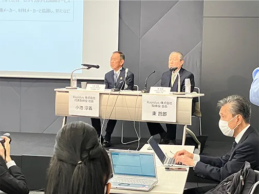
Director and Chairman: Tetsuro Higashi
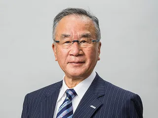
Representative Director and CEO: Dr. Atsuyoshi Koike (Engineering)
Leadership
Board of Directors
-
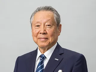 Director and ChairmanTetsuro Higashi
 -
 Representative Director and CEOAtsuyoshi Koike
 -
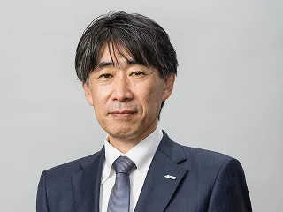 Representative Director,
Senior Managing Executive Officer,
Head of Operations DivisionAtsuo Shimizu -
 Director in charge of Legal and
ComplianceMakoto Matsuo -
 Director,
Senior Managing Executive Officer,
CFO and Head of Corporate DivisionAtsuko Murakami -
 Outside DirectorEmiko Higashi
 -
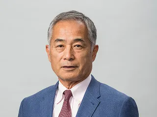
 Outside DirectorYoshimitsu Kobayashi
 -
 Outside DirectorMitsunobu Koshiba
 -
 Outside DirectorYoshio Nishi
 -
 Outside DirectorSiva Sivaram
 -
 Outside DirectorJohannes Stork
As of March 14, 2025
Corporate Auditor
- Corporate Auditor
- Yutaka Takeuchi
- Corporate Auditor
- Yasuhiko Yamato
As of March 14, 2025
Office Locations
- Tokyo Headquarters Office
-
Kojimachi Diamond Bldg., 4-1 Kojimachi, Chiyoda-ku, Tokyo 102-0083, Japan
- Chitose Office
- NTT Chitose Bldg., 2-16 Chiyoda-cho, Chitose-shi, Hokkaido 066-0062, Japan
- IIM-1
- 758-62 Bibi, Chitose-shi, Hokkaido 066-0012, Japan
- Rapidus Chiplet Solutions
-
758-173 Bibi, Chitose-shi, Hokkaido 066-8787, Japan
(Inside the Seiko Epson Corporation’s Chitose Plant) - Rapidus Design Solutions
- 3945 Freedom Circle, Suite 920, Santa Clara, CA 95054, USA

History of Rapidus
Rapidus Corporation was established in August 2022 to create advanced semiconductor and packaging technologies. Our mission is to improve efficiency, reduce power and improve the ecological impact of advanced computing in datacenters, autonomous vehicles, industrial manufacturing and artificial intelligence.
The digital society is advancing rapidly. AI will accelerate the need for more computation in datacenters, cars, factories and in our homes.
Semiconductors are an indispensable component for making business more adaptable, communications more reliable, transportation safer, and entertainment more available.
For this reason, semiconductors are now recognized by governments as strategic materials for their country’s economy and security. New foundries are needed to secure a stable supply of semiconductors.
Based on this recognition, it is extremely important for Japan to manufacture innovative logic semiconductors to support the world’s demand.
2022
Rapidus Corporation was established.
Rapidus has been selected for the "Next Generation Semiconductor R&D Project" by "Nedo" the New Energy and Industrial Technology Development Organization.
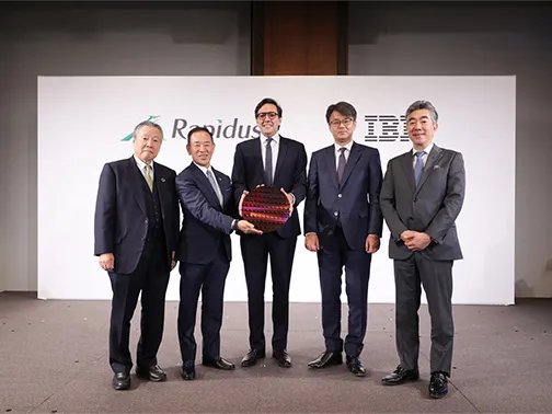
Rapidus has entered into a strategic partnership with IBM.
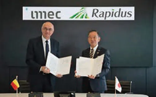
Rapidus has signed a MOU (Memorandum of Understanding) with imec.
The LSTC was established as a national R&D center aimed at realizing mass production technology for next-generation semiconductors.
2023
Rapidus announces it will build the "IIM" a new manufacturing facility in Chitose, Hokkaido
Joined imec's Core Partner Program
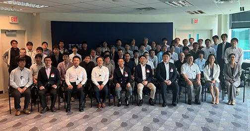
Rapidus has started dispatching engineers to IBM Albany at the Albany Nanotech Complex in New York, USA.
Rapidus held a briefing session on next-generation semiconductor projects and construction plans in Chitose, Hokkaido.
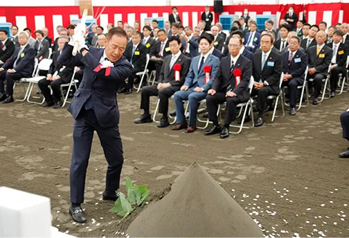
Rapidus held a groundbreaking ceremony at Chitose "Bibi World," the planned site of IIM-1, and began construction.
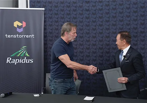
Rapidus has agreed to an IP partnership with US company Tenstorrent.
2024
Rapidus has opened its Chitose office.
Rapidus has announced a collaboration with Tenstorrent to develop and manufacture edge AI accelerators.
Rapidus has established a sales office, Rapidus Design Solutions, in Silicon Valley, USA.
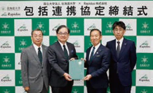
Rapidus has signed a comprehensive partnership agreement with Hokkaido University.
Rapidus has opened a Back-end processing R&D center within Seiko Epson's Chitose facility.
Rapidus has started the installation of Japan's first EUV exposure tool suitable for mass production, the NXE:3800E, at the IIM.
2025
PFN, Rapidus, and SAKURA internet have reached a basic agreement toward Japan-made AI infrastructure for a Greener Society.
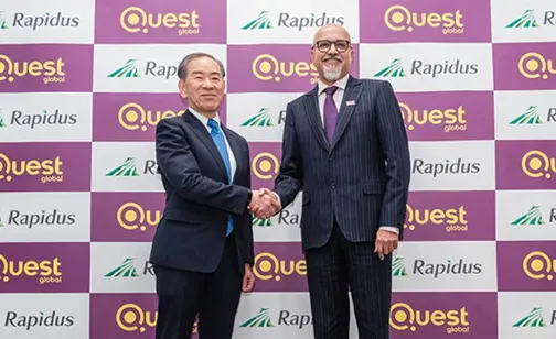
Rapidus has announced strategic partnership with Quest Global to enable Advanced 2nm Solutions for the AI chip era.
Rapidus starts operating the pilot line in IIM-1.
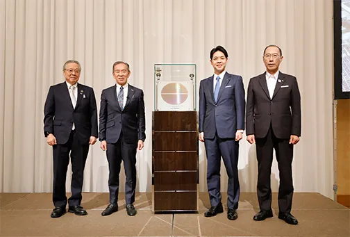
First prototypes of leading-edge 2nm GAA transistors successfully demonstrated electrical characteristics in IIM-1.
2027
Rapidus will begin mass production of next-generation logic semiconductors.