Business and Technologies
Business Overview
Rapidus consistently operates with a global perspective, promoting diversity and breaking down organizational barriers to constantly challenge innovation and provide the world's fastest cycle times.
The company is a semiconductor manufacturer that conducts research, development, design, manufacturing, and sales of electronic components such as semiconductor devices and integrated circuits, under a management policy of collaborating with world-class design companies, equipment manufacturers, and material suppliers to establish new business frameworks.
The following solutions are fully utilized to develop innovative logic semiconductors for mass production:
Rapidus core technology enables the production of advanced logic semiconductors which holds the key to solving tomorrow’s challenges
Rapidus is taking on the challenge of solving business and social challenges with semiconductor technology. We would like to introduce the core technologies that make this vision a reality.
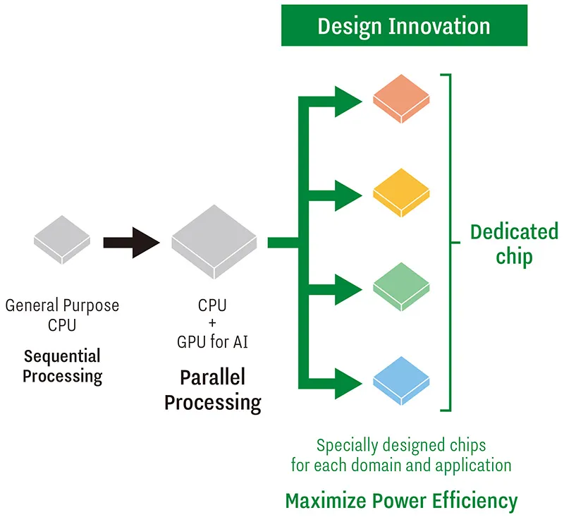
With the advent of the AI era, semiconductor foundries are required to operate more efficiently and manufacture a wider variety of products than ever before.
A transition to more advanced nodes and a new generation of semiconductor manufacturing processes will reduce the power required for AI training and inference.
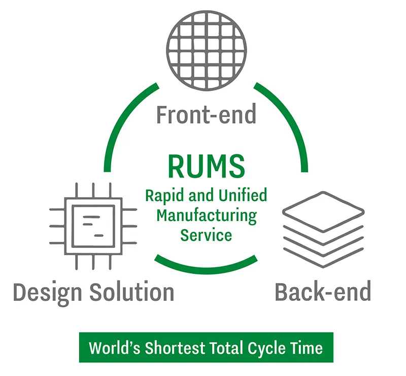
"RUMS" provides semiconductor design solution and integrated front-end and back-end processes
The current semiconductor industry is undergoing a horizontal division of labor.
- Fabless companies focus on semiconductor design. They do not own or operate manufacturing.
- Foundries which are commissioned by a fabless company to run the "front-end process" that manufactures the Si circuit on a wafer.
- Packaging which runs the “back-end process” of cutting and putting the Si circuit into a semiconductor chip.
Rapidus is a foundry which will provide a new business model called RUMS (Rapid and Unified Manufacturing Service).
With RUMS, our goal is to deliver state-of-the-art dedicated chips and chiplets using the GAA process to customers with the world's fastest cycle times.
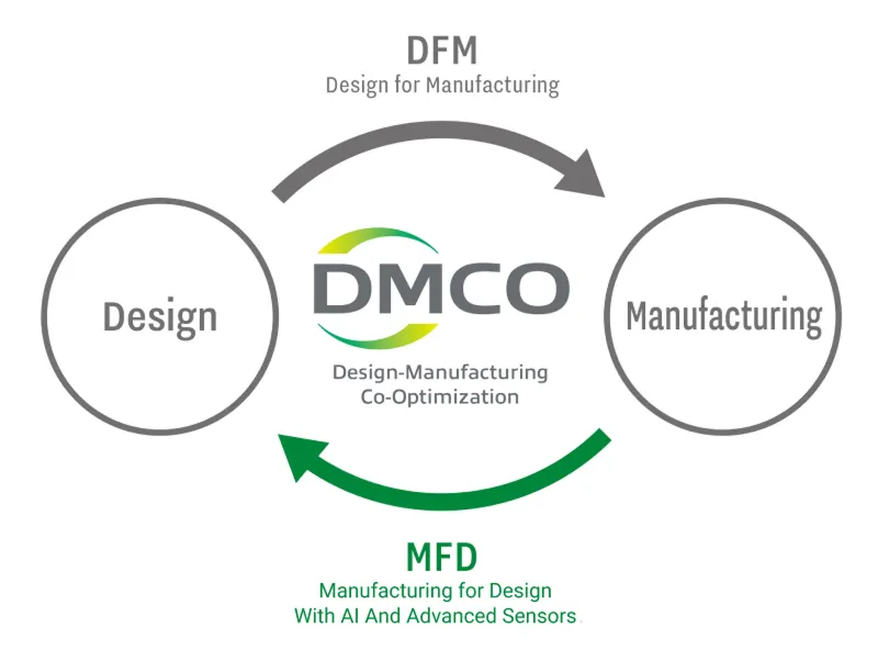
“Raads” supports design optimization using AI, and “DMCO” aims to mutually optimize design and manufacturing
Raads is a system operations platform developed by Rapidus and is based on machine learning models. By leveraging Raads' components, IIM enables mutual optimization of design and manufacturing, significantly reducing design time.
Sensors and AI will be used in the wafer process (front-end process) to improve design efficiency based on silicon big data obtained during the manufacturing process.
Manufacturing and quality data is analyzed by Raads: (Rapidus AI-Agentic Design Solutions). The output is shared with our fabless customers to help accelerate their design process. We call this “Manufacturing for Design.”
By combining the conventional DFM (Design for Manufacturing), and the Rapidus MFD (Manufacturing for Design), our IIM foundry delivers to our customers optimized designs and rapid manufacturing at the same time, enabling agile design for Manufacturing and Co-Optimization.
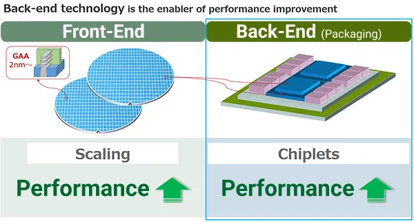
“GAA for the front-end process and “chiplets” for the back-end process were developed to deliver the world's fastest cycle time.
During the front-end process, a single 300mm (12”) wafer is manufactured, one at-a-time. Using single wafers allows more data to be collected for comprehensive data sets which enable ramp to mass production more quickly. Data captured in the Single Wafer model is used to feed it back for future designs. This is RUMS.
RUMS will drive significant improvement in yield in a shorter period. In addition, the single-wafer process can flexibly respond to the production of a wide variety of specialized products.
The Rapidus 2nm process will use a GAA (Gate All Around) transistor structure, which will deliver ultramodern, high-performance, low-power, dedicated AI chips to customers in a short period of time.
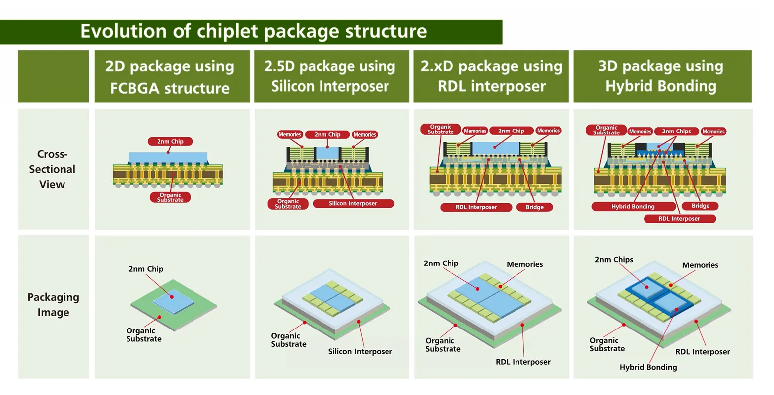
In the back-end process, we develop our own chiplet technology, in which the elements that make up the semiconductor are individually designed and later combined into a single product. Furthermore, by integrating the front-end and back-end processes, we aim to achieve the world's shortest total cycle times.
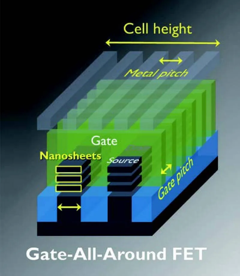
GAA(Gate-All-Around)
Maximizing Performance and Power Efficiency with the Rapidus Chiplet Solutions
Improvements to semiconductor system performance have traditionally been achieved through semiconductor circuit miniaturization in front-end technologies.
However, applications such as artificial intelligence (AI) require performance enhancements that exceed the current pace of semiconductor miniaturization.
To meet these demands, advanced packaging and heterogeneous integration are essential.
They are enabling back-end technologies to continue to evolve alongside front-end innovations, ensuring that the performance and efficiency of semiconductor devices continue to advance.
As AI chips evolve from general-purpose CPUs and GPUs to highly specialized devices and accelerators, the ability to provide customized solutions becomes critical.
Customization is also driving the adoption of chiplets.
Integration of multiple chiplets and functionalities within the package is driving
the need for larger packages.
By 2030, semiconductor package sizes are expected
to be two to three times larger than today and will require innovative packaging
solutions.
Rapidus is preparing to support its customers with a comprehensive range of capabilities and services: from design to state-of-the-art manufacturing of both front-end and back-end technologies that can address a wide range of processors.
Rapidus is developing advanced chiplet packaging solutions within its back-end technologies, to enable a seamless integration and assembly of multiple chiplets within a single package.
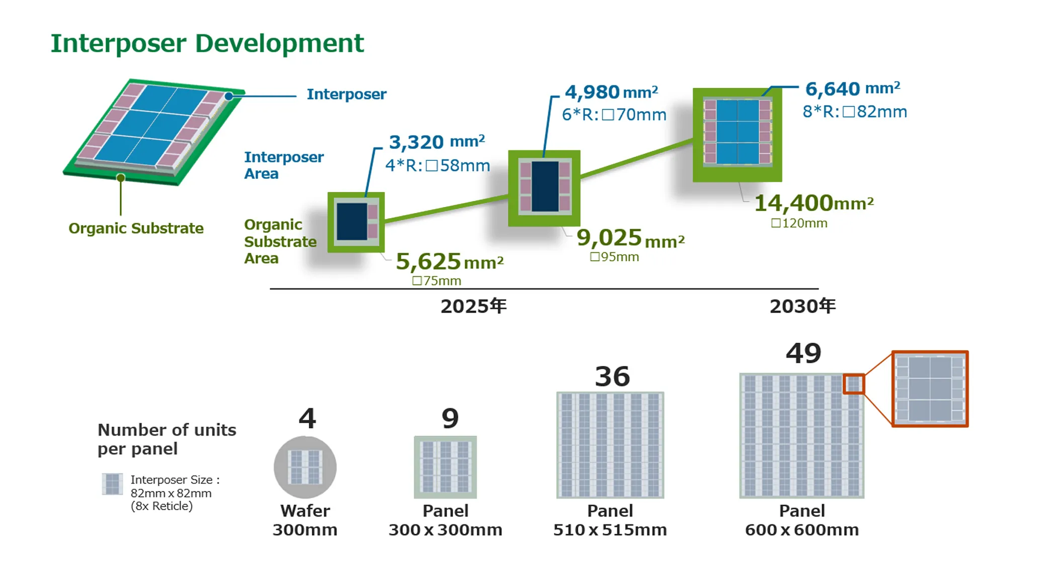
One example of Rapidus’ packaging advancements is development of one of the industry's largest 600mm square panel-level packaging technologies for more efficient production of high-performance and large packages.
In addition, to further improve performance and reduce power consumption, Rapidus is actively working on 3D chip stacking to enable shorter and denser inter-chip interconnects.
Rapidus is preparing a full suite of high-end performance packaging technologies needed to address the integration of next generation semiconductor devices.
Chiplet Package that Balances High Performance and Low Power Consumption
Demand for the next generation of logic semiconductors
In a rapidly evolving digital society, the adoption of AI, autonomous driving, smart cities, and robotics are increasing demand for advanced semiconductors.
Rapidus is addressing technology, business and social challenges through cutting-edge logic semiconductor technologies.
Next-generation semiconductors are indispensable for autonomous driving, AI, smart city concepts, robotics, and more.
State-of-the-art logic semiconductors are the foundation of digital technology, performing complex logic operations within advanced integrated circuits (ICs) to control the behavior of digital devices and systems, such as facial recognition, computation, communications, and various sensors.
A new generation of advanced semiconductors must meet high performance, low power consumption, miniaturization and other requirements,

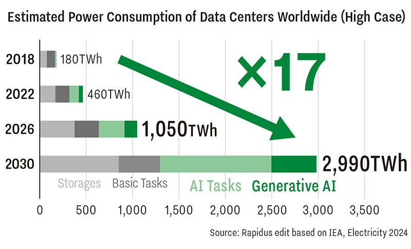
Demand for computing has increased dramatically, and electricity consumption has also increased.
With the advent of Generative AI, new services have appeared. Including real-time translation tools, image generation, autonomous vehicles to smart speakers. GenAI can generate sentences, create images and interact with people.
AI requires a huge amount of data and a huge amount of computation to train models and perform the AI service. Big data evolves AI, and AI creates big data.
This is predicted to dramatically increase the demand for computation, with global data creation projected to exceed 175 zettabytes in 2025, 612 zettabytes in 2030, and 2,000 zettabytes in 2035, up from 47 zettabytes in 2020. As a result, the power consumption of data centers around the world is expected to increase several times compared to the current level.
The biggest challenge is the power consumption of AI semiconductors.
Foundries for AI semiconductors must have faster production speeds and support a wider variety of products more than ever before.
A transition to ultramodern semiconductor manufacturing processes will help reduce the power required for AI training and inference. By moving from current generation chips to a 2nm process, the power cost of the same chip can be reduced by 1/4. At the same time, the miniaturization of semiconductors improves the performance of devices.
Today's AI servers are loaded with a large chip called a GPU and a large amount of memory called DRAM.
Services that utilize GenAI are currently being built using general-purpose semiconductors. To reduce power consumption and improve performance, semiconductors will be designed for each use case. Today, it takes time to design, develop, test and yield mass-produce semiconductors. Now more than ever, newer generations of more efficient and workload specific processors must come to the market.
It is expected 2nm processes and the adoption of dedicated-use-chips instead general-purpose semiconductors or “GPUs.” will reduce datacenter power consumption and speed computation times.