Technology
Introducing the cutting-edge semiconductor technologies and initiatives that Rapidus is working on.
-
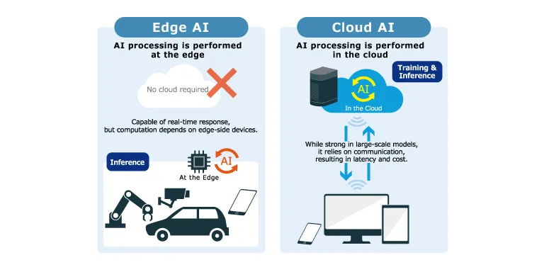 2026.01.26 What Is Edge AI? How the Latest AI Trends Are Tied Closely to Semiconductors
 -
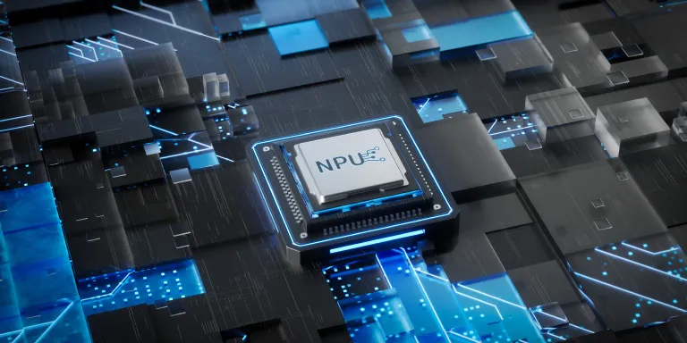 2026.01.26 What is an NPU? Understanding the Differences Between CPUs, GPUs and NPUs
 -
 2025.12.23 The Future Unlocked by Semiconductors: Innovation Expanding into Tomorrow
 -
 2025.12.23 What Are Semiconductors Used For? How They Work and Why They Underpin Modern Society
 -
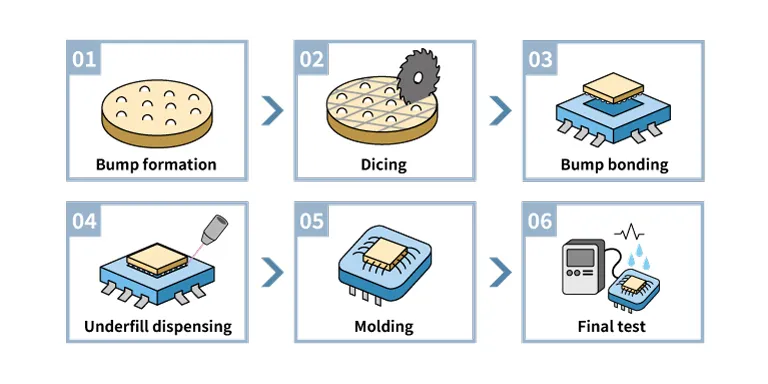 2025.11.28 The Semiconductor Back-End Process Explained: A Complete Picture of Product Packaging
 -
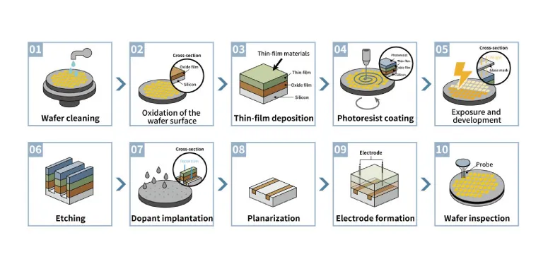 2025.11.28 Semiconductor Front-End Processing: An Overview of Nanoscale Manufacturing Steps
 -
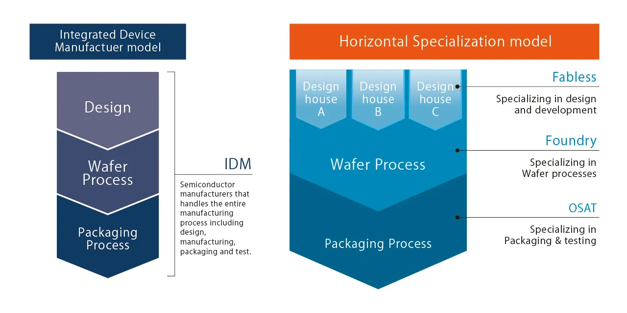 2025.10.24 What Is A Foundry? The Hidden Hero Of Semiconductor Manufacturing
 -
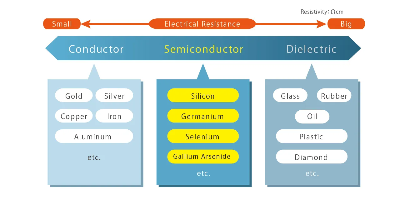 2025.10.24 What Are Semiconductors And Why Are They So Vital For Modern Innovation?
 -
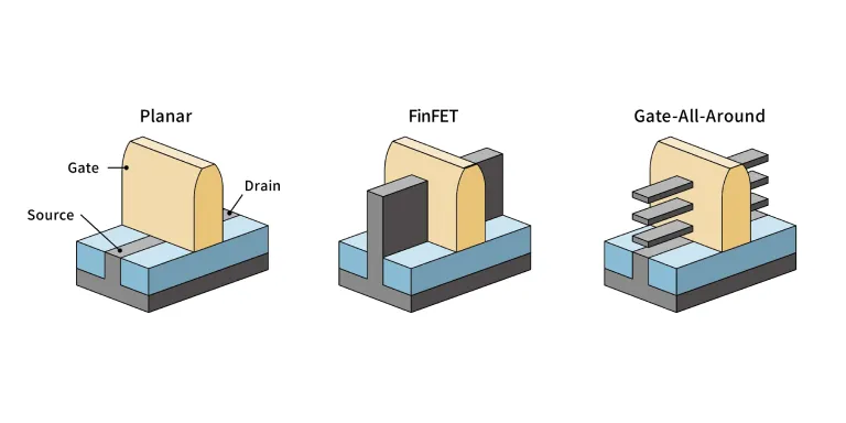 2025.09.10 2nm semiconductor challenges: Exploring Rapidus’ technological breakthroughs
 -
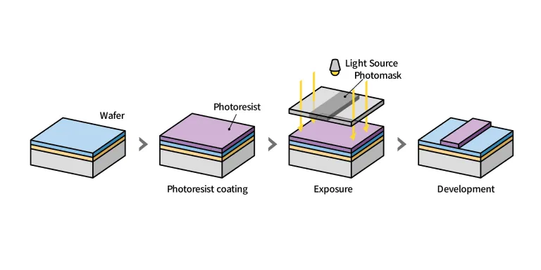 2025.09.10 What is EUV lithography? How this cutting-edge technology is powering Rapidus' next-gen semiconductor advancements
 -
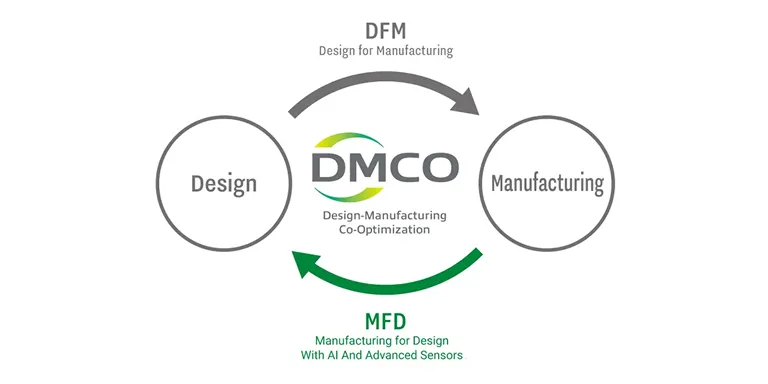 2025.07.11 Why is Semiconductor Design So Hard? – A Behind-the-Scenes Look at Rapidus' High-Speed Chipmaking Process
 -
 2025.07.11 What are AI Semiconductors? Power Problems in Data Centers and Game-Changing Technology
 -
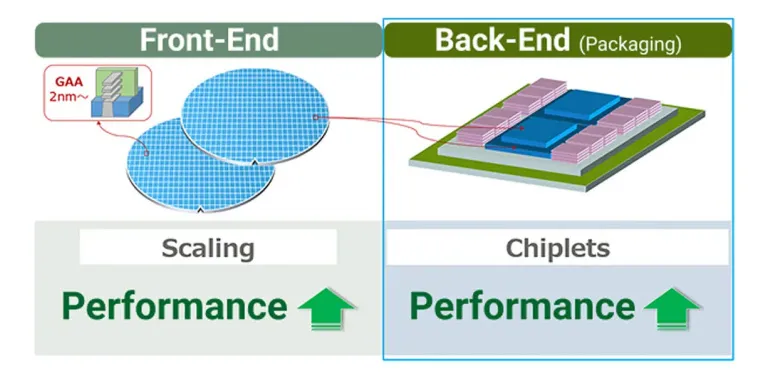 2025.07.02 What are Chiplets? - The Key Technology Behind Next-Gen Semiconductor Manufacturing
 -
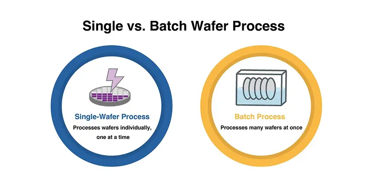 2025.07.11 Rapidus' Vision: 100% Single-Wafer Processing for Next-Generation Chip Manufacturing